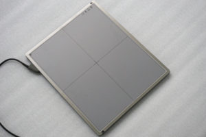
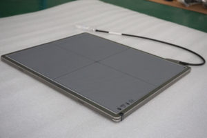
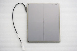
luminescent crystal layer, the X–ray photon energy is converted into visible light photon emission, and the visible light excites the photodiode to generate current. The current is integrated over the capacitance of the photodiode itself to form a stored charge. The amount of stored charge per pixel is proportional to the amount of incident X–ray photon energy in the corresponding range.
2 sulfur oxidation (Gd2O2S) + a-Si (amorphous silicon) + TFT: The X–ray photon to visible light conversion process is completed by using the sensitization screen material Gd2O2S.
3 cesium iodide ( CsI ) / bismuth oxysulfide ( Gd2O2S ) + lens / optical fiber + CCD / CMOS : X–ray first through the scintillator or phosphor visible light conversion screen, X–ray photons into visible light image, and then passed The lens or optical fiber sends the visible light image to the optical system, which is acquired by the CCD and converted into an image electrical signal.
4 CsI (Gd2O2S) + CMOS: This type of technology is limited by the poor spatial resolution of indirect energy conversion. Although a large number of low-resolution CMOS probes are used to form a large-area matrix, it is not able to effectively compete with the TFT panel.
Author:Alina
Tel:+86 18953679166
Email:service@newheek.com
Company:Weifang Newheek Electronic Tech Co., Ltd.